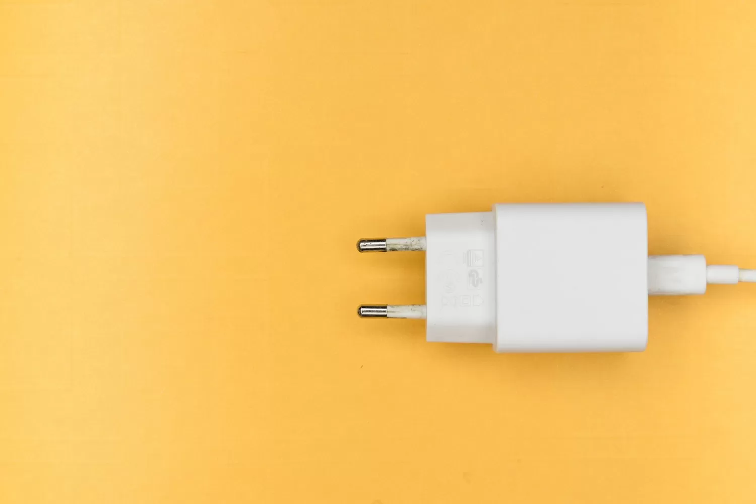
USB-C with Power Delivery has become the universal charging language — which means nearly every new product is either a PD sink (drawing power) or a PD source (providing it). The electrical design is well-trodden, but the difference between a charger that works and one that earns its certification is in the details of negotiation, conversion topology, and thermal honesty.
Negotiation: the conversation decides the design
PD is a protocol conversation on the CC line: source advertises fixed tiers (5/9/12/15/20 V) and PPS (programmable supply) ranges; the sink requests what it wants and can re-request dynamically. Design consequences:
- Sink side: a PD sink controller handles the protocol and drives the converter's feedback — ENCHIP(能芯) ECP-series PD take-off controllers are built exactly for this role, negotiating up to the higher PD3.x/PPS tiers and steering a downstream buck or buck-boost. PPS support is what separates "fast" from "fastest": PPS lets the load walk the voltage in 20 mV steps, minimizing conversion loss for a given battery state.
- Source side: advertise only tiers your thermal and topology budget can sustain. A 20 W design advertising 20 V/3.33 A must actually deliver it at 45 °C ambient in the smallest enclosure marketing will tolerate — under-advertising tiers is safer than failing a compliance soak test.
Topology: when buck-boost beats buck
A plain buck handles 20 V-to-battery when battery voltage stays below the input floor. But a 1–4S battery span or PPS-driven variable input makes the converter's job a true buck-boost: output regulation must hold through input dips and battery rise. The 4-switch buck-boost is the standard answer; its efficiency troughs (typically 90–93% near the transition region) set the thermal design point. ETA(钰泰半导体) converter and charging-management ICs slot into these power paths across the common voltage tiers, with companion LDOs and load switches for the housekeeping rails.
The thermal chapter you cannot skip
- Loss budget per stage. At 30 W with 92% efficiency, 2.4 W becomes heat in an enclosure the size of a deck of cards. Map each loss (FET conduction, switching, magnetics, rectification) and verify against θJA from the layout you will actually pour copper for — a 2-layer board with 1 oz copper is not the datasheet's 4-layer JEDEC board.
- Connector and cable current limits. The USB-C receptacle and the cable's CC-based current advertisement (3 A default vs 5 A with e-marker) bound the design before any FET does. Design the input path for the tier you negotiate — including the inrush and connector contact rating.
- Derating is a feature. Stepped current reduction as temperature climbs (PPS makes this protocol-native) turns a thermal limit into graceful behavior instead of a shutdown event.
Compliance and the long tail
USB-IF compliance aside, the field reality is a jungle of legacy cables, cheap sources, and protocol quirks. Robust products: soft-start every voltage transition, tolerate unexpected disconnects on CC, and log negotiation events (over that SPI NOR logger from your other subsystem) so field returns come back with data instead of anecdotes.
The domestic power-IC ecosystem now covers the full charger chain — ENCHIP negotiation controllers, ETA conversion and management silicon — at appliance-grade cost structures. The engineering work has shifted from sourcing scarce controllers to disciplined thermal and protocol design; the parts are the easy part.
Recommended next steps
If you are sourcing any of the parts mentioned in this guide, we can help you confirm stock, pricing, and lead times quickly.
- Upload your BOM — send your full parts list and receive a consolidated quote within 2 business hours.
- Browse related in-stock lines: Power Management ICs · Interface Chips / RF Chips.
- Contact our team for hard-to-find or end-of-life components.