Why the high-performance tier behaves differently
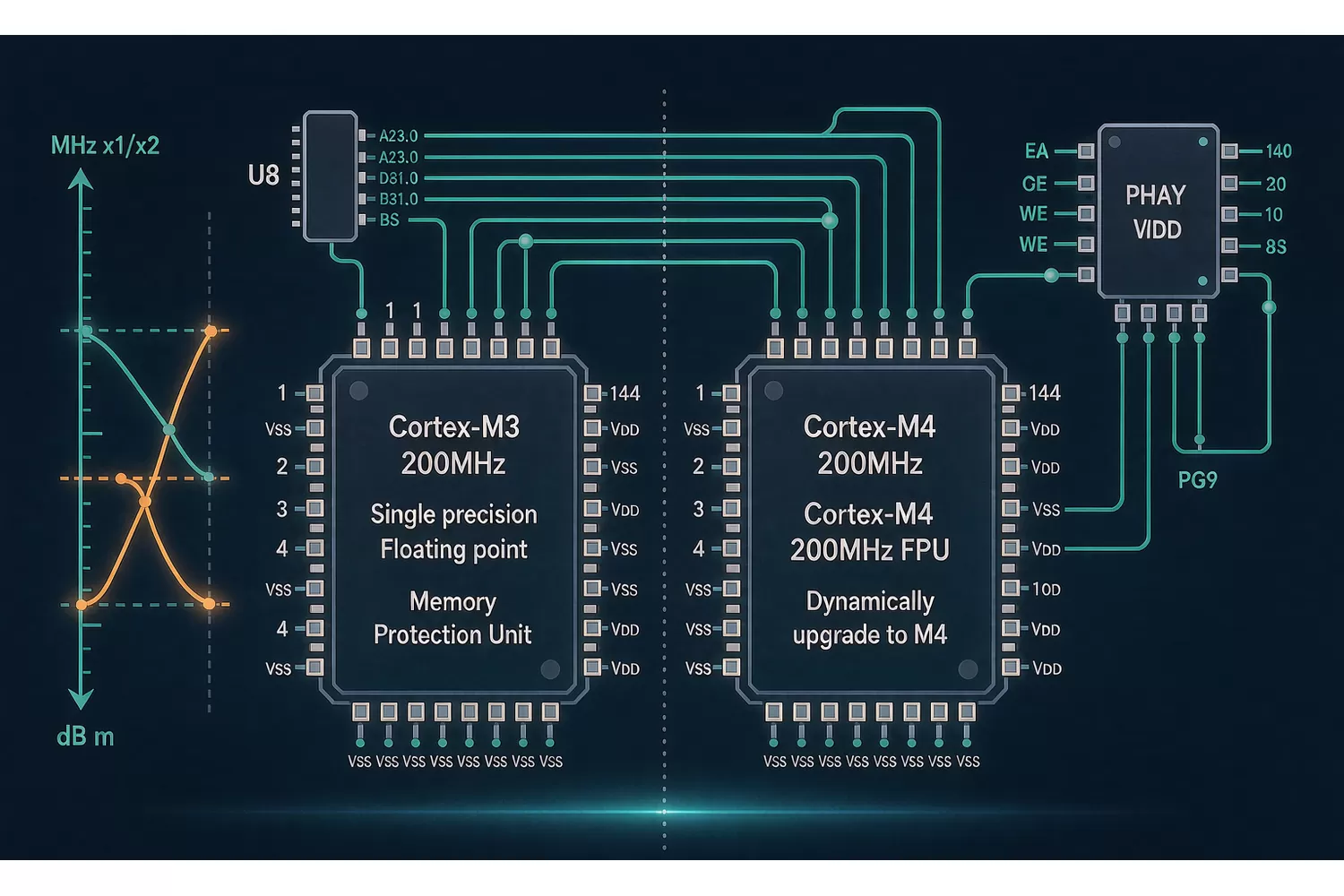
Swapping a small Cortex-M0 or M3 part is mostly a pinout and firmware job. Swapping a high-performance M4 is different, because these parts are usually the centre of a board that carries an external memory bus, an Ethernet PHY, a display interface or a camera, and a clock tree that everything else is timed from. The higher the integration, the more of the board moves with the MCU.

That does not make the move a bad idea. It means the qualification effort should be planned around the buses and clocks, not around the core.
The closest part-number pairings
| Design starting point | Closest AT32 counterpart | Typical package match |
|---|---|---|
| STM32F407ZGT6 (144-pin) | AT32F437ZGT7 | LQFP144 |
| STM32F407VGT6 (100-pin) | AT32F437VGT7 | LQFP100 |
| STM32F405 / F407 mid-density | AT32F435 series | LQFP64 / LQFP100 |
| STM32F429 with SDRAM / LCD-TFT | AT32F437 series | LQFP144 / LQFP100 |
| General-purpose F4 mid-tier | AT32F403A / AT32F407 | LQFP48 to LQFP100 |
Package count is the first filter, not the last. Two parts in the same LQFP144 body can still differ in which pin carries which alternate function.
What actually has to be re-verified
1. External memory interface timing
If the original design drives SDRAM or a parallel SRAM, the memory controller setup is the first thing to re-tune. Read and write latency, the refresh interval and the address/data hold timings are register fields with different defaults. Budget bench time with a logic analyser rather than assuming the existing values transfer.
2. Clock tree and PLL planning
Reaching the top of the frequency range usually needs a specific crystal and PLL combination. Confirm the crystal you already have on the board can produce an acceptable system clock, and check the USB and Ethernet clock paths separately — they have their own dividers and jitter requirements.
3. Ethernet MAC and PHY interface
An RMII PHY is the common case. Check whether the alternate function pins for the RMII signals and the 50 MHz reference clock land on the same package positions. If they move, it is a layout change, not a firmware change.
4. DMA channels and peripheral instances
DMA request mapping is rarely one-to-one. Code that hard-codes a DMA channel number for a UART, SPI or ADC will need the mapping table revisited — this is the single most common source of "it compiles but the transfer never completes" during a swap.
Firmware effort, honestly
| Work item | Small design | Board with memory bus + Ethernet |
|---|---|---|
| Startup and linker files | hours | hours |
| Clock and PLL reconfiguration | 1 day | 2-3 days including timing validation |
| DMA request remapping | hours | 1-2 days |
| Driver-level peripheral port | 1-3 days | 3-5 days |
| External memory tuning | not applicable | 3-7 days on the bench |
| Board re-layout | none if pin-compatible | likely for PHY and memory routing |
These are planning ranges, not quotes. The point is the shape: the core migration is cheap, the memory bus and PHY are what consume the calendar.
When this replacement makes sense, and when it does not
- Makes sense: a new board revision is coming anyway; the memory bus is not heavily loaded; you need a second source for a part with a long lifecycle ahead.
- Makes sense: the design is display or control heavy and the existing part is oversized for the job, giving headroom to step down a tier later.
- Think twice: the product is in volume production with a validated EMC file and no planned revision. The re-testing cost can exceed the unit saving.
- Think twice: the design depends on a peripheral that has no direct counterpart, where the workaround costs more code than the migration itself.
Parts in this tier that we hold stock on include AT32F437ZGT7, AT32F435ZGT7, AT32F437VGT7 and AT32F435VMT7. For a step-down before committing to the big package, the mid-tier AT32F435CGT7 is worth putting on the bench first. Everything is listed under Microcontrollers / MCUs.
Verify before you commit: pinout, peripheral mapping and electrical limits differ between part numbers and between silicon revisions. Always confirm against the current official datasheet and errata for the exact order code you intend to use.
Questions & Answers
Is the AT32F437 pin-compatible with an STM32F407?
Not automatically. Same package size does not guarantee the same pin function. Build a pin-by-pin table of every signal you actually use before you commit, and check the alternate-function mapping for each one.
How long does a high-performance MCU swap take?
The firmware port is usually days. The calendar time is dominated by external memory timing, PHY routing and EMC re-testing, which can run into weeks if a board revision is required.
Do I need to re-tune the SDRAM controller?
Treat it as required. Controller defaults differ, and margin that was tuned for one silicon revision does not carry across. Verify setup, hold and refresh timings on the bench.
What is the most common mistake during this kind of swap?
Assuming the DMA channel mapping is identical. It rarely is, and the failure looks like a silent hang rather than a compile error.
Recommended next steps
If you are sourcing any of the parts mentioned in this guide, we can help you confirm stock, pricing, and lead times quickly.
- Upload your BOM — send your full parts list and receive a consolidated quote within 2 business hours.
- Browse related in-stock lines: Microcontrollers / MCUs · Interface Chips / RF Chips.
- Contact our team for hard-to-find or end-of-life components.
About us & trademarks: Jingteng Electronics (Shenzhen Jingteng Electronics Technology Co., Ltd.) is an independent distributor of electronic components. We are not an authorised distributor, agent or representative of any manufacturer named in this article. Manufacturer names, part numbers and trademarks are used for identification and technical compatibility only and belong to their respective owners.