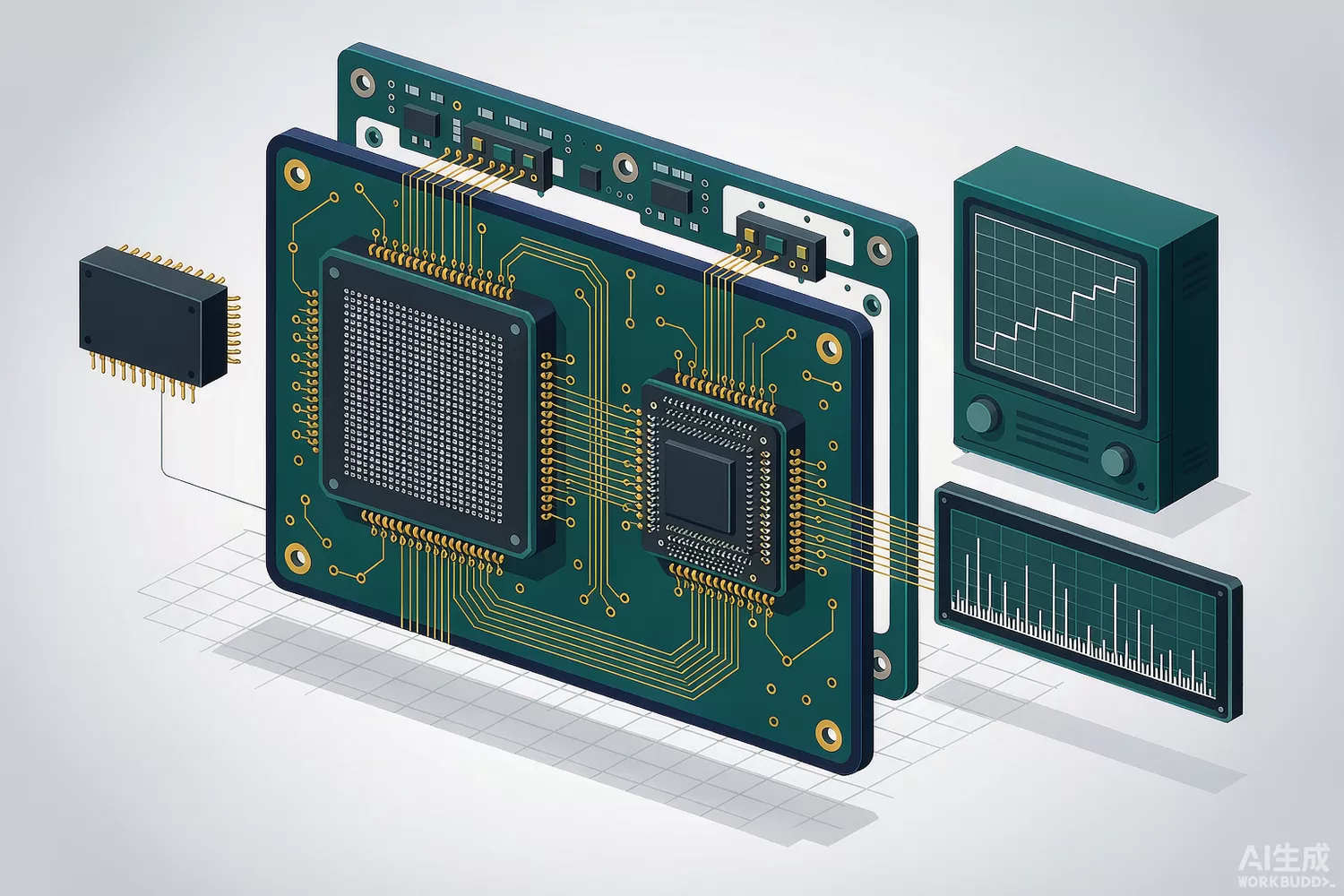
Direct digital synthesis (DDS) generates a waveform by stepping a phase accumulator and reading a sine table into a DAC. Given one good clock, the output frequency becomes an exact rational fraction of that clock with microhertz-class resolution, and frequency, phase and amplitude are all programmable in real time. That combination — precision, agility and parameter control — is why DDS sits at the heart of signal generators, frequency-hopping excitors, coherent radar waveform sources and impedance-analyser stimulus chains. This article explains the selection logic, the recent technology moves, and the state of domestic alternatives to the Analog Devices AD98xx family.

Application logic: when a DDS beats a PLL
A PLL locks to discrete channels and moves in microseconds to milliseconds; a DDS retunes in a handful of clock cycles with phase continuity. Use a DDS when you need any-frequency agility (sweeping, hopping, chirp), independent control of phase and amplitude, or sub-hertz resolution. Use a PLL when you need wide tuning range at high frequency with low spur count. Many practical excitors chain the two: a DDS provides a low-frequency agile reference that a PLL multiplies to RF — a structure covered in our PLL and VCO article.
The classic single-chip anchors are the AD9851 (125 MHz-class clock, simple parallel/serial control), the AD9854 (300 MHz clock, dual orthogonal 12-bit DACs, FSK/BPSK/chirp modes) and the AD9858 (up to 180 MHz output with an on-chip charge-pump PLL). Their mix of phase accumulator width, DAC resolution and modulation modes decides which fits a design.
Datasheet parameters that decide success
- Maximum clock and output bandwidth (typically 40–45% of the clock before the reconstruction filter).
- Frequency resolution set by the accumulator width (32-bit is roughly 0.03 Hz at a 125 MHz clock; 48-bit reaches microhertz).
- Spurious-free dynamic range near your output frequency — DAC truncation spurs cluster there, not at the headline figure.
- Phase noise: DDS output phase noise tracks the clock plus a 20 log(N) penalty from the reference multiplier, so a clean clock multiplier strategy matters.
- Amplitude and phase register depth for fine control (AD9854-class parts give 12-bit amplitude and 14-bit phase control).
- Control interface and update rate for hopping and chirp profiles.
New technology in synthesis
The current generation has moved in two directions. Upward, wideband multi-channel converters with embedded synthesizers pair 14–16-bit DACs running at gigasample rates with direct digital synthesis of carriers into the hundreds of megahertz and JESD204B-style serial data interfaces, so one clock tree synchronises many transmitters. Downward and sideways, MCU-plus-DAC and FPGA constructions now cover the low end: a 32-bit microcontroller driving an SPI DAC, or an FPGA phase accumulator feeding a high-speed DAC, reproduces DDS behaviour where integration into existing logic is more valuable than a dedicated chip.
Domestic alternatives: status and indicative cost
Public domestic capability here is still largely at family and solution level rather than catalog-listed single-chip. China Electronics Technology Group Corporation entities publish related building blocks: CETC's listed chip platform (stock code 600877) has announced series-production-grade frequency-synthesizer and divider circuits up to 30 GHz and 20 GHz integrated-VCO synthesis families, and Chengdu Huada Microelectronics (Chengdu Huada) exhibits high-speed clock and AD/DA signal-chain families — its CSD6952 high-speed clock driver supports up to ten channels at 17 GHz — alongside FPGA and precision-DA product lines. In practice, domestic designs implement AD9854-class functionality either with an FPGA plus a high-speed domestic DA, or with CETC-family synthesizer circuits in defence-adjacent programmes, and validate spurious performance board by board. For cost planning the comparison is therefore architecture versus chip.
Price figures below are indicative public-market reference ranges for moderate volumes, compiled from publicly observable listings. They fluctuate with the spot market, package option, grade (industrial, automotive, screened) and order quantity, and must not be read as a quotation. Ask us for a firm price on your exact part numbers and quantities.
| Function (imported anchor) | Example import part | Indicative import price (USD) | Domestic candidate | Indicative domestic price (USD) |
|---|---|---|---|---|
| 125 MHz-class DDS, single output | AD9851 (Analog Devices) | 8.00 – 15.00 | MCU + SPI DA construction (for example GD32/MCU plus domestic DA) | 1.50 – 4.00 (BOM) |
| 300 MHz dual-quadrature DDS with modulation | AD9854 (Analog Devices) | 20.00 – 45.00 | FPGA + high-speed DA solution; CETC synthesizer families (family level) | 8.00 – 25.00 (BOM) |
| DDS with on-chip PLL reference | AD9858 (Analog Devices) | 15.00 – 30.00 | CETC 600877 frequency-synthesizer series (family level) | 10.00 – 30.00 |
| Clean analog rail for the DAC | TPS7A4700RGWR (TI) | 2.00 – 3.50 | HX2001 LDO / COS29xxx LDO families | 0.20 – 0.80 |
| Control MCU / trim DAC around the synthesizer | STM32F407VGT6 + MCP4725A0T | 4.00 – 7.00 | GD32F303CBT6 + domestic DA | 1.00 – 2.50 |
The honest gap is documentation of measured wideband spurious behaviour, as public engineering discussion of AD9854-class substitutions notes: low-frequency purity tracks closely, while upper-band spurious performance depends heavily on power-integrity design. Budget prototype iterations for that reason.
Validation flow
Drive the candidate at your real clock with your real reconstruction filter, read SFDR across the planned output band on a spectrum analyser, and check phase-continuous switching time with an oscilloscope in infinite-persistence mode. Compare against the AD98xx part on the same board — layout and clocking dominate differences more than silicon. If your need is a fixed-frequency multi-output clock rather than an agile waveform, the any-frequency clock generator approach is cheaper still.
Frequently asked questions
Why is my DDS output noisier at higher frequencies?
Because output phase noise picks up a 20 log(N) penalty when the reference multiplier multiplies the clock, and because DAC images and truncation spurs rise relative to a falling wanted signal. Improve the clock, avoid the on-chip multiplier, and filter close to the clock fundamental.
Can an FPGA replace a dedicated DDS chip?
For logic-heavy systems yes: an FPGA phase accumulator plus a fast DAC reproduces the architecture and integrates with your control plane. You take on the design work the chip vendor had already done, especially spurious management.
Is a domestic single-chip AD9854-class part available?
Public catalogues currently document domestic capability at family or solution level (CETC synthesizer families, high-speed DA plus FPGA constructions) rather than as an openly catalogue-listed single-chip equivalent. Treat published part claims with care and request measured SFDR data.
What clock quality does a DDS need?
The DDS output inherits the clock's phase noise. Use a low-noise crystal or TCXO reference and a low-noise regulator; the DDS cannot clean a dirty clock.
About us & trademarks: JTDZ Tech (Shenzhen Jingteng Electronics Technology Co., Ltd.) is an independent distributor of electronic components. We are not an authorised distributor or representative of the imported manufacturers named in this article. Manufacturer, brand and part names are used for identification purposes only; all trademarks remain the property of their respective owners. Cross-reference information in this article is based on publicly available sources, is subject to change, and is not a substitute for your own engineering validation. Always verify specifications against the manufacturer's datasheet before design-in or purchase.