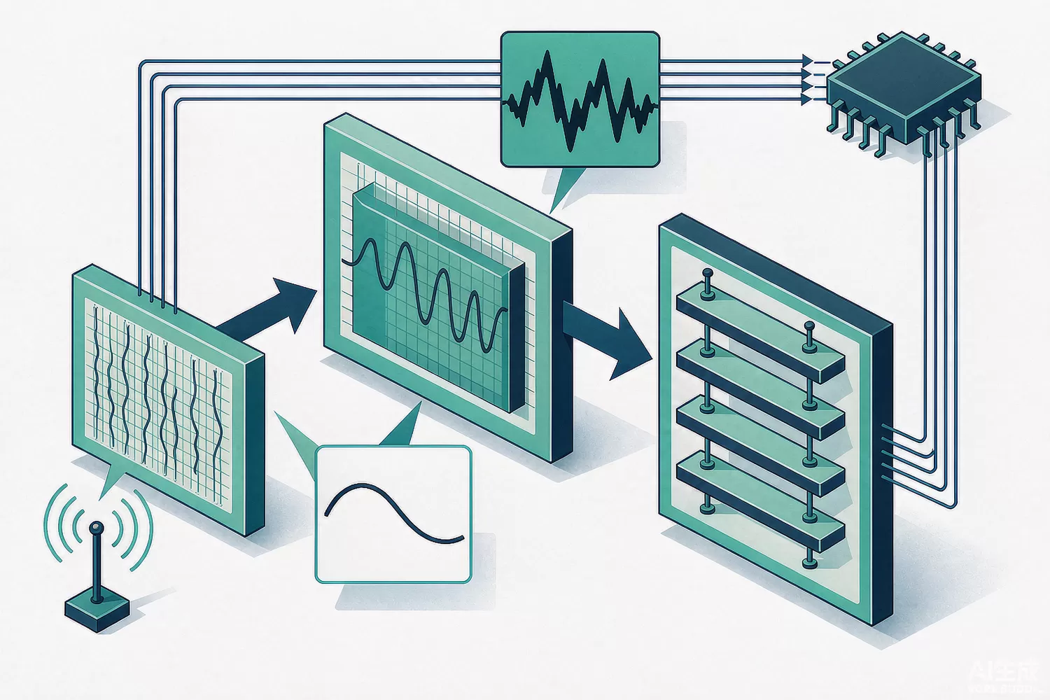
Every radio that must work with signals of wildly different strength needs an automatic gain control loop, and almost every AGC loop contains the same quiet workhorse: the digitally controlled attenuator or variable-gain amplifier. It is the part that lets a receiver survive a nearby transmitter, lets a test instrument set a level repeatably, and lets a beam-forming channel hold its calibration while its neighbours change state. It is cheap, it is easy to underestimate, and it is one of the RF functions where domestic parts are fully competitive.

Application logic: where the gain control sits and why
The physical position of the attenuator in the chain is a system decision, not a layout detail. Placed early, before the first high-gain stage, it controls the level at the most vulnerable node and therefore protects the whole receiver from compression; placed late, it sets the level presented to the demodulator or the converter and gives the cleanest absolute accuracy. Many designs use two devices — a coarse front-end attenuator for protection and a fine one near the converter for level setting — which is why multi-stage, low-step-size parts exist. What must not happen is a chain where the only gain control sits after a stage that is already in compression: at that point the information is gone and no downstream attenuation recovers it.
The parameters that matter are attenuation range, step size and monotonicity of the transfer characteristic, insertion loss at minimum attenuation (which appears directly in the receiver noise figure), input third-order intercept and compression point at each setting, switching speed and switching transient behaviour, and the control interface. That last one deserves a warning: parallel or serial control lines crossing the RF area can inject noise and spurs, so devices with internal decoding, fast settling and clean state changes are worth their small premium. For the same reason, designers treat the attenuator and the front end as one problem — the same reasoning behind using attenuators and limiters to protect a front end and the loss budgeting in insertion-loss accounting.
In phased arrays and multi-channel instruments, the requirement changes shape. Here the attenuator is a calibration element: every channel needs independent, repeatable gain control with known step accuracy and known phase behaviour, because a gain change that also shifts phase corrupts the beam. That is why arrays specify gain-control parts with low phase variation versus attenuation, not only low insertion loss.
New technology in gain control
- GaAs and SOI digital step attenuators with 0.25 dB steps and serial or parallel control, offering wideband coverage from DC to above 6 GHz in small QFN packages.
- Serial-addressable architectures that let several attenuators share one control bus, which reduces the pin count in multi-channel boards.
- Glitch-free switching design, where the internal state changes without amplitude spikes, removing the transient that used to disturb demodulators.
- Temperature-variable attenuators and compensation networks that flatten gain drift in wide-temperature equipment without digital intervention.
- Integrated variable-gain amplifiers that combine the attenuation network and the amplifier on one die, cutting part count in compact radios.
- Digital pre-distortion and closed-loop level control implemented in the host, which allows simpler analogue gain blocks while keeping the transmitted level accurate.
Domestic alternatives: what to analyse before switching
- Compare insertion loss at minimum attenuation first: it is the figure that lands directly in your noise-floor calculation.
- Check the attenuation accuracy and monotonicity at each bit, at your frequency band, and over temperature.
- Confirm control-interface timing and the state on power-up. A device that powers up in minimum attenuation can expose your front end during boot.
- Ask for switching transient data if your modulation is sensitive to amplitude glitches.
- Verify the linearity at each attenuation state; intercept points often change with the setting.
- For array designs, request phase variation versus attenuation, which is rarely on the first page of a datasheet and always matters.
Indicative cost comparison: imported originals vs domestic candidates
Price figures below are indicative public-market reference ranges for moderate volumes, compiled from publicly observable listings. They fluctuate with the spot market, package option, grade (industrial, automotive, screened) and order quantity, and must not be read as a quotation. Ask us for a firm price on your exact part numbers and quantities.
| Device class | Common imported reference | Indicative imported unit price | Commonly referenced domestic candidate | Indicative domestic unit price |
|---|---|---|---|---|
| 6-bit digital step attenuator, DC–6 GHz, 0.25–0.5 dB steps | pSemi PE43xxx series; ADI / Hittite DSA families; Mini-Circuits DAT series | USD 3–12 | Bonray BR9032FL / BR9606FP-class digital gain-control devices; additional domestic GaAs DSA families | USD 1.2–5 |
| Digital variable-gain amplifier, 500 MHz–4.2 GHz, 31.5 dB range | Qorvo QPB0066-class digital VGA modules | USD 6–18 | Bonray BR9606FP-class 6-bit digital VGA (0.5 dB step, 31.5 dB range) | USD 2.5–8 |
| Analogue voltage-controlled amplifier (RF/IF AGC) | ADI AD603-class voltage-controlled amplifier | USD 6–14 | COS603VGA-class voltage-controlled amplifiers (Cosine) | USD 2.5–7 |
| Temperature-variable / PIN-diode attenuator | EMC Technology TVA and MTVA series; Avago / Broadcom PIN attenuators | USD 4–10 | Domestic temperature-compensated and PIN attenuator families | USD 1.5–5 |
Two cost notes. First, digital step attenuators are one of the clearest domestic wins in the RF BOM: the function is well defined, the specification is measurable, and the domestic parts are often a genuine like-for-like replacement in the same package family. Second, do not let the attenuator's price drive the architecture. A cheaper device with 0.5 dB more insertion loss may cost you a whole extra gain stage, a change that dwarfs the saving on the part itself.
Commonly referenced alternative models
| Imported original (reference) | Domestic candidate (public sources) | Why it is referenced |
|---|---|---|
| pSemi PE43711 / PE43610 — serial and parallel digital step attenuators | Domestic GaAs DSA families with 0.5 dB steps, published by Chinese MMIC suppliers (e.g. Bonray's digital gain-control line) | Same function and comparable control structure; compare bit accuracy and insertion loss in your band. |
| Qorvo QPB0066-class digital variable-gain amplifier, 5–500 MHz | Bonray BR9606FP (500 MHz–4.2 GHz, 6-bit, 0.5 dB step, 31.5 dB range, QFN24) | Publicly documented as a wideband digital VGA with 0.5 dB steps and a documented intercept point; note the frequency coverage differs, so check your band. |
| Mini-Circuits DAT-31575-series digital step attenuator | Domestic 6-bit parallel-control digital VGAs and DSAs in QFN packages | Cross-referenced as functionally corresponding gain-control elements; the control interface may be parallel rather than serial, which changes board wiring. |
| ADI AD603-class voltage-controlled amplifier | COS603VGA-class voltage-controlled amplifier (Cosine) | Publicly documented as a low-noise, rail-to-rail voltage-controlled amplifier aimed at RF/IF AGC, video gain control and instrumentation, with a linear-in-dB gain law. Verify gain range and bandwidth in your loop. |
| Avago / Broadcom ALM-38140 PIN-diode attenuator | Domestic PIN-diode attenuator families (MMIC suppliers and discrete PIN diode vendors) | Same role in level control and protection; the PIN approach is slower but very linear and is often preferred in transmit paths. |
We stock digital step attenuators, PIN attenuators, temperature-variable attenuators and the gain blocks around them, including the PE43610A-X digital step attenuator, PE43711B-Z, DAT-31575-SP+ from Mini-Circuits and ALM-38140 PIN-diode attenuator, plus the pSemi collection, Mini-Circuits collection and the wider RF and interface chip collection.
Frequently asked questions
Frequently asked questions
Why is a digital step attenuator better than a variable-gain amplifier?
A digital step attenuator is calibrated by design: each bit is a switched resistive or FET element with a defined attenuation value, so the setting is repeatable from unit to unit without calibration. A variable-gain amplifier is continuous and cheaper in some bands, but its gain law drifts with frequency, temperature and supply, and it usually needs factory calibration in products that care about absolute level.
What are the most common mistakes in an AGC design?
Putting the attenuator after the last high-gain stage so that the loop cannot protect the front end; ignoring the switching transients, which appear as amplitude glitches in the demodulator; forgetting that the control interface itself can radiate into the RF path; and specifying attenuation range without checking the insertion loss at zero attenuation, which sets the receiver's noise figure floor.
How many bits do I need?
It depends on how tightly the loop must hold the level and how much dynamic range it must cover. A six-bit, 0.5 dB-step device gives 31.5 dB of range, which suits most receive AGC loops; test and instrumentation chains often want 0.25 dB steps over a wider range, and multi-stage attenuators are used where the total range exceeds what one device can cover.
Do you stock attenuators and the surrounding chain?
Yes. We quote digital and analogue attenuators, temperature-variable and PIN-diode types, plus the gain blocks, switches and filters around them, from imported brands and from domestic suppliers. Tell us the frequency band, the attenuation range, the step size and the interface you want and we will come back with options and indicative pricing.
About us & trademarks: JTDZ Tech (Shenzhen Jingteng Electronics Technology Co., Ltd.) is an independent distributor of electronic components. We are not an authorised distributor or representative of the imported manufacturers named in this article. Manufacturer, brand and part names are used for identification purposes only; all trademarks remain the property of their respective owners. Cross-reference information in this article is based on publicly available sources, is subject to change, and is not a substitute for your own engineering validation. Always verify specifications against the manufacturer's datasheet before design-in or purchase.