What the calculator does not know
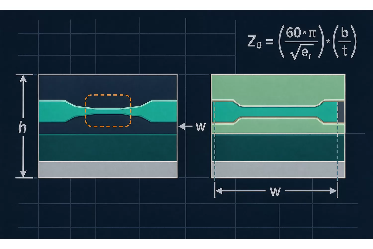
A trace impedance calculator needs three inputs: the dielectric constant and thickness of the board material, the trace width, and the distance to the reference plane. What it does not know about your board is the copper weight after etching, the fact that the etched width is narrower than the nominal artwork, the solder mask that now covers the trace and changes the effective dielectric, and the via stitching pattern that turns a gap in the ground plane into a slot in the ground plane. Each of those moves the impedance by a few percent, and a few percent across a quarter-wave section is a meaningful phase and reflection error.

The errors that actually cost dB
The most expensive RF layout mistakes are rarely the trace width. They are: a ground plane with a slot under the trace, a via that returns the current poorly and adds inductance in series with the signal, a filter components pad that is one size too small for its own lead inductance, a ground via placed a millimetre away from the shield footprint of a packaged part, or a component placed so that its pad is part of the matching network without being simulated as such. Every one of these is a lumped or distributed error that the schematic never sees.
What good looks like on the bench
Measure the return loss at the reference plane of your connector, not at a test point on the board. If the trace has been tuned with the datasheet's evaluation board as a reference, first check whether your board build matches the evaluation board's stack-up. If it does not, expect the evaluation measurements to be optimistic. Then verify with a vector network analyser that the impedance matches across frequency rather than at a single spot frequency.
A short checklist before you panelise
| Check | Typical mistake | Effect |
|---|---|---|
| Ground return path | Slot in the plane near the trace | Added inductance and loss |
| Via stitching | One via instead of a row | Poor return, drifting impedance |
| Copper weight | Assumed 1 oz, built 2 oz | A few percent off target |
| Solder mask | Not accounted for | Small but consistent shift |
| Component pads | Oversized ground pads | Parasitics the schematic ignores |
| Reference plane | Mixed dielectric stack-up | Impedance far off target |
When to stop chasing impedance
At frequencies below a few hundred megahertz, a well routed trace with a solid ground is usually good enough and the calculated impedance matters less than tidy layout. Above roughly 1 GHz the same trace can behave differently, and at millimetre-wave frequencies the entire package and the antenna feed become part of the circuit. The useful mental model is that the board is part of the design, and that part has tolerances.
Nothing in this article removes the need for measured parts. Our stock covers the passive and active RF parts that most of these layouts use, including Mini-Circuits LFCN-4400+ low-pass filter for the match and decouple sections, pSemi PE42462A-X where switching has to be placed close to the antenna feed, and the RF and interface parts listed under Interface / RF Chips.
Questions & Answers
Why does my measured impedance differ from the calculator?
Copper etching narrows the trace, the solder mask adds a dielectric layer, and the impedance formula you used probably assumed ideal copper and a perfect plane. Each deviation shifts the result a little.
Does solder mask really change impedance?
It adds a dielectric on top of the conductor, which raises the effective permittive coupling and lowers impedance slightly. On dense RF boards it is a measurable effect.
How many ground vias does a shielded RF part need?
A row immediately around the shield footprint is the usual guidance. A single via or a via far from the part leaves the shield ineffective and lets the parasitics dominate.
At what frequency does trace length start to matter?
Above roughly a fifth of the wavelength, meaning around 300-400 MHz for a 40 mm trace on a typical laminate, trace length starts to behave as transmission line rather than as a connecting wire.
Related RF Components & Articles
- Browse our full range of RF chips & RF components.
- Related pSemi (Murata) parts: pSemi (Murata) components.
- Related Mini-Circuits parts: Mini-Circuits components.
- Looking for LFCN-4400? Check stock and specs on the product page.
- Looking for PE42462A-X? Check stock and specs on the product page.
- Related article: Power Amplifier Compression: The Real Cost of Pushing Past 1 dB.
- Related article: RF Attenuators and Limiters: Protecting the Front End Without Killing Sensitivity.
- Need pricing or availability? Upload your BOM or contact our team.
Recommended next steps
If you are sourcing any of the parts mentioned in this guide, we can help you confirm stock, pricing, and lead times quickly.
- Upload your BOM — send your full parts list and receive a consolidated quote within 2 business hours.
- Browse related in-stock lines: Interface Chips / RF Chips.
- Contact our team for hard-to-find or end-of-life components.
About us & trademarks: Jingteng Electronics (Shenzhen Jingteng Electronics Technology Co., Ltd.) is an independent distributor of electronic components. We are not an authorised distributor, agent or representative of any manufacturer named in this article. Manufacturer names, part numbers and trademarks are used for identification and technical compatibility only and belong to their respective owners.