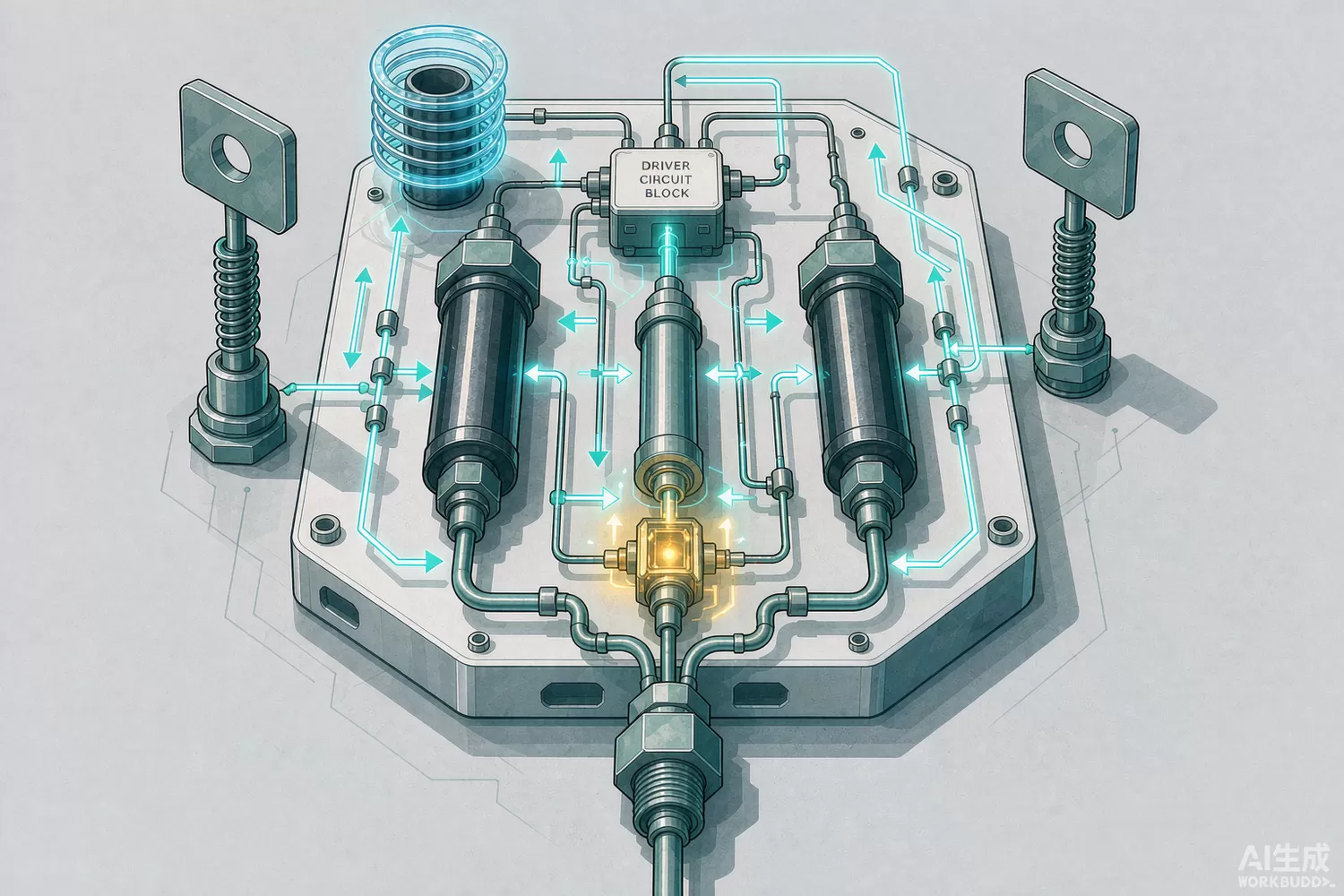
A PIN diode is a nearly ideal RF switch element: under forward bias its I-layer floods with carriers and looks like a small resistor; under reverse or zero bias it is a small capacitor. Because the RF behaviour is set by stored charge rather than by a junction acting as a rectifier, a properly driven PIN diode switches signals of tens or hundreds of watts with negligible distortion — something no SOI or CMOS switch IC can survive. This article focuses on externally driven, watt-class switching: antenna changeover, filter banks, duplexing and transmit-path switching. (Self-acting protection is a different job; see our PIN limiter article, and for small-signal IC switching see the RF switch IC guide.)

Application logic: series, shunt and SPDT topologies
In a series switch, the diode conducts the signal path; insertion loss is set by its on-resistance Rs, so high-power series diodes (the MACOM MA4P class, e.g. MA4P7447 and MA4P7002F) are specified by Rs at your drive current and by carrier lifetime. In a shunt switch, the diode shorts the line when on; isolation is set by off-state capacitance, so a low-Cj diode with high breakdown wins. Real designs combine both: an SPDT antenna switch uses two series arms plus shunt stubs, achieving 30 dB-plus isolation while passing 50 W. Filter banks use one shunt diode per filter branch, so only the selected branch is connected — the diode count scales with filter count, not with power.
The driver is half the design
PIN switching fails in the driver more often than in the diode. The forward current must be large enough that stored charge exceeds the RF current amplitude — a common rule is If ≥ 10× the peak RF current divided by 2π times the carrier lifetime. Too little current and the diode rectifies the RF, generating distortion products. The bias tee that injects DC into the RF path needs a choke with enough RF impedance at your lowest frequency, and the DC block needs low capacitance at your highest. Switching speed is governed by carrier lifetime: fast switching (microseconds) wants short-lifetime parts such as the HSMP-3890 class, while brute-power switching tolerates longer-lifetime dies.
Choosing the diode: three families, three jobs
- General-purpose SMT switching diodes — Skyworks AS179-92LF and NXP BAP64-03: low cost, single-supply drive, ideal up to a few watts in antennas and filter banks.
- Fast, low-capacitance switch diodes — Broadcom HSMP-3890 and QSMP-4810: microsecond switching and good isolation through the low-GHz bands.
- High-power stud and chip PINs — MACOM MA4P7447, MA4P7002F, MA4P282 and the dual MA4P274CK: tens of watts of CW with controlled Rs, for duplexing and high-power filter switching.
New technology: driver integration and high-voltage control
Two refinements define current practice. First, integrated PIN drivers that sequence bias rails and sink the charge-storage current are replacing discrete transistor drivers, trimming switching transients that previously upset PA bias. Second, higher-voltage I-layer processing pushes the same SOT-23 footprint to 200 V-plus breakdown, letting one package cover both the series and shunt roles of a 100 W switch. On the systems side, PIN diodes coexist with GaN switch ICs: the diode handles raw power, the IC handles logic and low-power routing, and the design splits the path accordingly. Skyworks' APD0510 illustrates the modern low-inductance SMT packaging that makes this split practical at board level.
Domestic alternatives: families and indicative cost
Domestic high-power PIN capability is documented at family level: China Electronics Technology Group Corporation research institutes (CETC-13 in Shijiazhuang and CETC-55 in Nanjing) publish high-power silicon PIN switching and limiting diode families in SOT-23, chip and stud formats, with Rs, carrier lifetime and breakdown data available through controlled channels. Commodity-grade switch diodes are also second-sourced by commercial domestic lines. Validate Rs at your drive current and distortion at your worst-case RF level — those two numbers, not headline breakdown voltage, decide success.
Price figures below are indicative public-market reference ranges for moderate volumes, compiled from publicly observable listings. They fluctuate with the spot market, package option, grade (industrial, automotive, screened) and order quantity, and must not be read as a quotation. Ask us for a firm price on your exact part numbers and quantities.
| Function (imported anchor) | Example import part | Indicative import price (USD) | Domestic candidate (family level) | Indicative domestic price (USD) |
|---|---|---|---|---|
| General-purpose SMT PIN switch diode | AS179-92LF (Skyworks) / BAP64-03 (NXP) | 0.10 – 0.40 | Domestic commercial PIN lines | 0.06 – 0.25 |
| Fast low-C switching diode | HSMP-3890 (Broadcom) | 0.30 – 0.90 | CETC-13/55 fast PIN families | 0.20 – 0.60 |
| High-power CW switching PIN, chip | MA4P7447 / MA4P7002F (MACOM) | 5.00 – 18.00 | CETC-13/55 high-power PIN families | 3.00 – 10.00 |
| Dual / stud configurations | MA4P274CK / MA4P282 (MACOM) | 6.00 – 25.00 | CETC-13/55 stud & dual families | 4.00 – 15.00 |
| Low-inductance SMT high-power PIN | APD0510 (Skyworks) | 0.50 – 1.50 | CETC-13 SMT PIN families | 0.30 – 1.00 |
High-power PIN diodes are qualified by measurement, not by substitution tables. Build the intended switch on your PCB, drive it at the planned current, and measure insertion loss, isolation, and third-order distortion at maximum RF power and at the temperature extremes — then switch sources on the same fixture.
Frequently asked questions
How much forward current does my PIN switch need?
Enough that stored charge exceeds the RF current: roughly If >= 10 x I(RF peak) / (2 x pi x lifetime). Undersized drive shows up as increased distortion, not as a failed switch.
PIN diode or GaN/SOI switch IC for a 50 W antenna switch?
For 50 W CW, PIN diodes remain the practical choice; IC switches top out far lower in power. Use the IC for low-power routing and the diode at the high-power node.
Why does my switch distortion rise at high RF power?
The diode is running out of stored charge and beginning to rectify. Increase drive current, choose a longer-lifetime die, or reduce the RF current by moving the switch to a lower-impedance point.
Are domestic high-power PIN diodes credible second sources?
Family-level documentation from CETC-13/55 indicates serious industrial capability. Qualify on R_s at your drive current and distortion at your RF level, on your own fixture.
About us & trademarks: JTDZ Tech (Shenzhen Jingteng Electronics Technology Co., Ltd.) is an independent distributor of electronic components. We are not an authorised distributor or representative of the imported manufacturers named in this article. Manufacturer, brand and part names are used for identification purposes only; all trademarks remain the property of their respective owners. Cross-reference information in this article is based on publicly available sources, is subject to change, and is not a substitute for your own engineering validation. Always verify specifications against the manufacturer's datasheet before design-in or purchase.